Product Summary
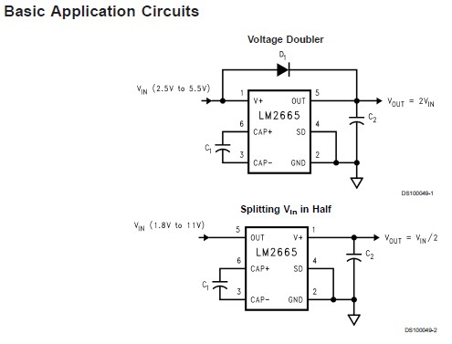
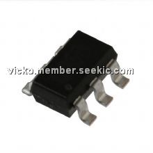
The LM2665M6X CMOS charge-pump voltage converter operates as a voltage doubler for an input voltage in the range of +2.5V to +5.5V. Two low cost capacitors and a diode(needed during start-up) are used in this circuit to provide up to 40 mA of output current. The LM2665M6X can also work as a voltage divider to split a voltage in the range of +1.8V to +11V in half. The LM2665M6X operates at 160 kHz oscillator frequency to reduce output resistance and voltage ripple. With an operating current of only 650 μA (operating efficiency greater than 90% with most loads) and 1μA typical shutdown current, the LM2665M6X provides ideal performance for battery powered systems. The device is in SOT-23-6 package.
Parametrics
LM2665M6X absolute maximum ratings: (1)Supply Voltage (V+ to GND, or GND to OUT): 5.8V; (2)SD: (GND - 0.3V) to (V+ +0.3V); (3)V+ and OUT Continuous Output Current: 50 mA; (4)Output Short-Circuit Duration to GND: 1 sec.; (5)Continuous Power Dissipation (TA = 25℃): 600 mW; (6)TJMax: 150℃; (7)θJA: 210℃/W; (8)Operating Junction Temperature Range: -40° to 85℃; (9)Storage Temperature Range: -65℃ to +150℃; (10)Lead Temp. (Soldering, 10 seconds): 300℃; (11)ESD Rating: 2kV.
Features
LM2665M6X features: (1)Doubles or Splits Input Supply Voltage; (2)SOT23-6 Package; (3)12W Typical Output Impedance; (4)90% Typical ConversioEfficiency at 40 mA; (5)1μA Typical ShutdowCurrent.
Diagrams

| Image | Part No | Mfg | Description |  |
Pricing (USD) |
Quantity | ||||||||||||
|---|---|---|---|---|---|---|---|---|---|---|---|---|---|---|---|---|---|---|
 |
 LM2665M6X |
 National Semiconductor (TI) |
 Charge Pumps |
 Data Sheet |

|
|
||||||||||||
 |
 LM2665M6X/NOPB |
 National Semiconductor (TI) |
 Charge Pumps |
 Data Sheet |

|
|
||||||||||||
 (China (Mainland))


